
Market Position and Market Share
Lasertec Corporation(TSE: 6920) is an indispensable global leader in semiconductor mask inspection and metrology, occupying an effective monopoly in actinic extreme ultraviolet(EUV) patterned mask inspection.
- Actinic EUV Patterned Mask Inspection: Lasertec commands an estimated 100% market share globally (ACTIS series, including A150/A300). It was the first company in the world to commercialize inspection systems that use the identical 13.5nm EUV wavelength as lithography scanners.
- EUV Mask Blank Inspection/Review: Holds a near-monopoly market share exceeding 90% (such as the ABICS and MAGICS series).
- Broad Photomask Inspection Market:In the overall global photomask inspection and review equipment market(estimated at JPY 300–400 billion), Lasertec ranks among the top 2 worldwide alongside KLA Corporation, holding 50% to 70% market share in Deep Ultraviolet(DUV)-based mask inspection tools.
- Silicon Carbide(SiC) / Compound Wafer Inspection: Lasertec ranks #1 to #2 globally with its SICA series, widely adopted by power semiconductor manufacturers for substrate defect identification.
Supply Chain Analysis and Key Suppliers
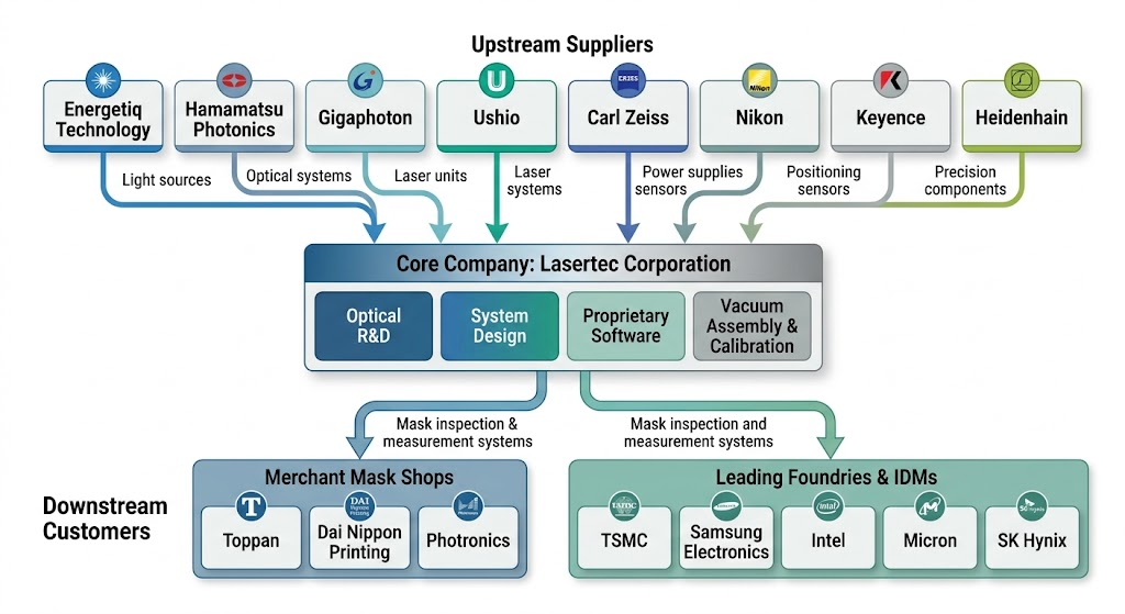
Lasertec operates an asset-light, fabless/fab-lite manufacturing and operational model. Internal resources concentrate almost exclusively on optical R&D, core system design, proprietary software algorithms, and final precision assembly/calibration, outsourcing standard mechanical machining and subsystem fabrication.
- Upstream Supply Chain:
- EUV Light Sources & Discharge Generators: High-energy EUV light sources require extreme stability and compact discharge-produced plasma(DPP) or laser-produced plasma(LPP) architectures. Key specialized partners include Energetiq Technology(a Hamamatsu Photonics subsidiary) for high-brightness short-wavelength light sources, as well as Gigaphoton and Ushio.
- Precision Optics & Mirrors: High-precision reflective multilayer mirrors(molybdenum-silicon Mo/Si coatings) and ultra-flat optics are critical for EUV beam guidance. Suppliers include specialized European and Japanese optical houses such as Zeiss, Nikon, Canon, and high-spec coating fabricators.
- Vacuum & Mechatronics Subsystems: Ultra-clean vacuum chambers, high-precision interferometers, piezo stages, and robotic mask-handling transfer arms designed to prevent particle contamination inside vacuum environments. These are procured from precision machinery partners such as Keyence, Heidenhain, and Japanese robotic handling OEMs.
- Sensors and Detectors: Ultra-sensitive EUV-grade TDI(Time Delay Integration) image sensors and detectors, custom-developed in collaboration with advanced sensor manufacturers such as Hamamatsu Photonics and Sony.
- Downstream Supply Chain:
- Merchant Mask Shops: Independent photomask manufacturers including Toppan Photomask, Dai Nippon Printing(DNP), and Photronics, who utilize Lasertec inspection tools to certify mask blank integrity and inspect patterned reticles before shipping.
- Semiconductor Foundries & IDMs: Advanced-node manufacturers who represent the core revenue base. Key accounts include TSMC, Samsung Electronics, Intel, and leading memory producers(Micron, SK Hynix), who deploy Lasertec systems for incoming mask verification and fab pellicle-mounted reticle monitoring during active lithography cycles.
Competitor Analysis: Technical and Financial Comparison
The primary global competitors in mask inspection and high-end process control are KLA Corporation(KLAC) and Applied Materials(AMAT).
- Technical Comparison:
- Actinic vs. Non-Actinic(E-Beam/DUV) Inspection: Lasertec’s decisive moat is its proprietary actinic(13.5nm EUV) optical architecture. It inspects through EUV pellicles and identifies phase defects that only manifest at the 13.5nm wavelength.
- KLA Corporation: The dominant titan in general wafer defect inspection and traditional optical mask inspection(Teron series). However, KLA’s leading-edge mask solutions rely heavily on advanced high-resolution DUV or multi-beam electron-beam(e-beam) approaches rather than native actinic EUV light. While e-beam provides microscopic resolution, its throughput is inherently slower compared to Lasertec’s full-field optical scanning.
- Applied Materials: Competes primarily with e-beam review and pattern verification systems(such as Aera series). AMAT provides high-throughput wafer inspection and metrology, but does not offer a direct actinic EUV photomask inspection platform comparable to Lasertec’s ACTIS.
- Financial Comparison:
- Operating Margin Profile: Lasertec maintains an extraordinary operating margin hovering around 40% to 50% (e.g., generating over JPY 120 billion in operating profit on ~JPY 250–290 billion in revenue), reflecting its pricing power and monopoly status in EUV. In comparison, KLA operates at a 38% to 42% operating margin, and Applied Materials generates around 29% to 31%.
- Revenue Scale & Diversification: KLA(~$10–12B annual revenue) and Applied Materials(~$26–28B annual revenue) possess broad, diversified product portfolios across etching, deposition, metrology, and wafer inspection. In contrast, Lasertec has a much smaller, highly concentrated top line(~JPY 250–290 billion, roughly $1.6–1.9B) that is directly tied to leading-edge advanced node CapEx cycles.
- Capital Efficiency: Lasertec achieves exceptionally high Return on Equity(ROE > 40%) driven by its fabless assembly model, low fixed-asset intensity, and negative working capital dynamics enabled by customer milestone advance payments.
Information Sources
- https://sharedresearch.jp/en/companies/6920/report/6528fd0394023d00164a11ad
- https://the-shashi.com/en/tse/6920/financials/
- https://www.hudson-labs.com/research/kla-competitors-klac-top-peers-in-2026
- https://www.lasertec.co.jp/en/products/microscope/optelics_hybrid/hardware/
back to Lasertec