
Corporate History
Foundational Period(1960–1980s): Optical Metrology and LSI Roots
Founded in 1960 in Yokohama as Tokyo Microphoto Laboratory by Yasushi Uchiyama, the company initially focused on precision optical equipment. In 1976, it launched the world’s first automatic mask inspection system for large-scale integration(LSI), establishing an early core competency in optical pattern defect detection. The company rebranded to Lasertec Corporation in 1986.
Diversification and Scanning Laser Technology(1990s–2000s)
During this phase, Lasertec expanded beyond photomask tools into scanning laser microscopes and flat panel display(FPD) photomask inspection. It went public on the JASDAQ market in 1990 and subsequently listed on the First Section of the Tokyo Stock Exchange in 2013. The firm strategically pursued niche optical inspection applications where competitors could not justify dedicated development.
The EUV Bet and Global Dominance(2010s–Present)
Anticipating extreme ultraviolet(EUV) lithography adoption when many incumbents considered actinic inspection commercially unviable, Lasertec committed heavy engineering resources to direct EUV light source inspection. In 2019, it introduced the ACTIS A150, the world’s first actinic EUV patterned mask defect inspection system. This established a near-monopoly that scaled rapidly with 7nm, 5nm, 3nm, and 2nm node transitions, cementing its position in global leading-edge semiconductor manufacturing.
Business Model and Strategy
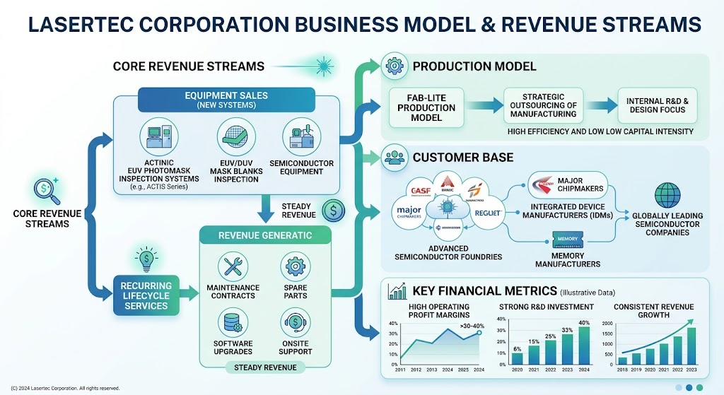
Lasertec generates revenue through two primary pillars: high-value capital equipment sales and recurring installed-base lifecycle services. Rather than acting as a volume hardware manufacturer, Lasertec operates a fab-lite model centered on proprietary R&D, optical architecture, and software, while outsourcing non-critical component fabrication.
In equipment sales, its flagship ACTIS systems command unit prices estimated between ¥5 billion and ¥8 billion(~$35M–$55M), driven by actinic 13.5nm wavelength illumination that detects phase defects embedded within multilayer mask blanks and patterned reticles. In FY2026(ended June 30, 2026), Lasertec posted net sales of ¥230.49 billion, with semiconductor-related equipment delivering ¥168.09 billion and recurring services contributing ¥58.65 billion(up 36.5% YoY).
The operating strategy centers on:
- Value-Based Monopoly Pricing: Operating margins reached 45.67%(¥105.26 billion operating profit in FY2026), reflecting immense pricing leverage where customers have no commercial actinic inspection alternative.
- Growing Recurring Revenue Base: As the cumulative installed base of EUV and DUV inspection platforms expands globally, long-term service agreements, field software upgrades, and laser maintenance yield predictable, high-margin cash flows.
- High-NA EUV Transition: Deploying High-NA(0.55 NA) inspection platforms to capture early qualification capex across next-generation node development.
Information Sources
- https://www.lasertec.co.jp/en/ir/plan/message.html
- https://sharedresearch.jp/en/companies/6920/report/6528fd0394023d00164a11ad
- https://the-shashi.com/en/tse/6920/financials/
- https://www.hdinresearch.com/news/1948
- https://umbrex.com/resources/company-profiles/lasertec-corp/
AI Development Strategy and Industry Collaborations
Lasertec treats artificial intelligence not as a standalone software product, but as an embedded capability within its inspection algorithms to tackle the diminishing signal-to-noise ratio in sub-2nm pattern verification.
R&D Allocation and Investment Scope
Lasertec allocates approximately 5% to 10% of its annual sales directly to research and development. In its medium-term plan through 2030, Lasertec targets baseline R&D reinvestment of approximately 10% of revenue(targeting ¥40 billion to ¥50 billion annually by 2030). A substantial portion of this software allocation is earmarked for AI-driven image processing, noise reduction, and automated defect classification(ADC).
Deep Learning Defect Classification(ADC)
At extreme lithographic dimensions, optical inspection captures tens of thousands of nuisance surface variations that do not affect transistor functionality. Lasertec integrates deep convolutional neural networks(CNNs) and deep learning models directly into the tool firmware. The algorithm classifies genuine printability defects(such as phase defects in Mo/Si multilayers or pellicle contamination) versus non-fatal optical noise in real time, drastically cutting reticle review cycle time for fab operators.
Collaborations and Industry Ecosystem
Because mask qualification requires close alignment with exposure optics, Lasertec collaborates closely with leading lithography ecosystem partners:
- EUV Consortium and Research Centers: Lasertec maintains joint technical evaluations with leading semiconductor research institutes, including Imec in Belgium, to validate defect printability models on advanced high-NA EUV test masks.
- Leading-Edge Customers: Deep proprietary collaboration with key clients(TSMC, Intel, Samsung) allows Lasertec to feed proprietary fab inspection data back into iterative training sets for its die-to-database and die-to-die inspection engines.
- Compute Hardware Integration: To handle gigapixel-per-second optical throughput from EUV cameras, Lasertec utilizes high-performance industrial computing clusters and GPU accelerated vision platforms to execute complex deep learning inference pipelines on-tool without throttling mechanical scanning speeds.
back to Lasertec