Foundational Years and Technological Genesis (1975-1996)
KLA’s origin traces back to two Silicon Valley pioneers, each possessing unique expertise in semiconductor inspection and measurement.
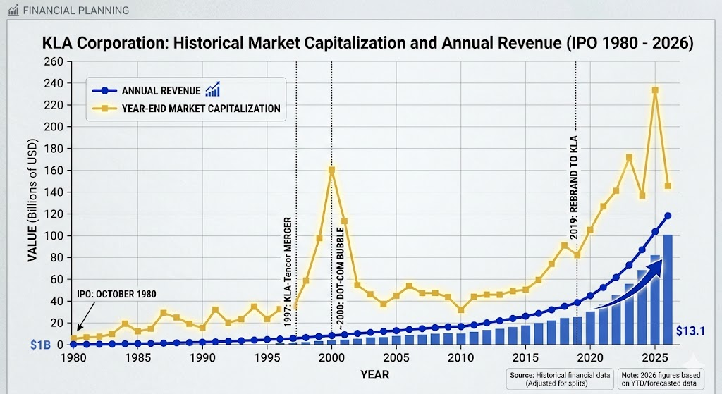
- 1975: Ken Levy and Bob Anderson founded KLA Instruments, focusing on automated photomask inspection using optical technology, which significantly advanced wafer fab productivity at the time.
- 1976: Dan Maydan founded Tencor Instruments, specializing in wafer metrology to measure thin-film thickness and surface flatness.
- During this period, both companies independently established the technical benchmarks for defect detection and measurement, setting the stage for modern process control.
Mega-Merger and Market Expansion (1997-2007)
As semiconductor manufacturing increased in complexity, the two industry leaders joined forces to provide an integrated solution.
- 1997: KLA Instruments and Tencor Instruments merged to form KLA-Tencor. This landmark merger united defect inspection and precision metrology, creating an unrivaled powerhouse in the process control market.
- Following the merger, the company pursued aggressive strategic acquisitions, incorporating key technologies in electron-beam (E-beam) inspection, optical critical dimension (CD) metrology, and reticle manufacturing tools to broaden its product portfolio.
Advanced Node Scaling and Global Consolidation (2008-2017)
As chip features shrunk below 20nm, traditional inspection methods encountered significant physical limitations.
- KLA-Tencor heavily invested in R&D, integrating advanced algorithms, computational optics, and big data analytics into its hardware. This enabled leading logic and memory manufacturers to overcome critical yield barriers during the early adoption of Extreme Ultraviolet (EUV) lithography.
- The company consolidated its position within the global semiconductor supply chain, standing alongside giants like ASML, Applied Materials (AMAT), and Tokyo Electron (TEL).
Rebranding, Diversification, and the AI Era (2018-Present)
To align with its expanding technology footprint and the demands of next-generation computing, the company entered its latest phase of evolution.
- 2019: The company officially rebranded as KLA Corporation to reflect its broader technological scope. In the same year, KLA completed the acquisition of Orbotech, expanding its expertise into printed circuit boards (PCBs) and flat panel displays (FPDs).
- With the industry shifting toward 3nm, 2nm, and sub-2nm nodes, alongside advanced 3D packaging, KLA integrated AI and machine learning into its systems. These technologies enable automated defect classification and predictive yield modeling, securing KLA’s role as a vital enabler of the ongoing artificial intelligence and high-performance computing (HPC) expansion.
KLA holds an absolute dominant position in the semiconductor process control and yield management market. According to recent data, KLA commands a 55% to 58% market share in this sector, demonstrating an exceptionally deep competitive moat.
The competitive landscape for KLA is analyzed below:
1. Core Competitive Advantages (Moat)
- Unrivaled Market Share and Ecosystem Lock-in: With over 50,000 active systems installed worldwide, KLA has accumulated decades of defect data and proprietary chip analysis algorithms. This creates extremely high switching costs for customers.
- Superior Profit Margins: Leveraging its technological monopoly, KLA consistently maintains its gross margin at a high level of 61% to 62%, with operating margins hovering between 36% and 42%, far outperforming the semiconductor equipment industry average.
- Robust, High-Margin Service Revenue: Post-installation maintenance, software upgrades, and optimization services account for nearly 25% of total revenue, providing an excellent anti-cyclical cash flow.
- Rising Process Intensity: As wafer manufacturing shifts toward advanced nodes below 2nm (such as GAA architectures) and experiences a boom in advanced packaging (like HBM and CoWoS), the share of inspection and metrology within Wafer Fab Equipment (WFE) spending has risen from 5.3% in 2019 to 7.4% currently, and is projected to reach 9% by 2030. This makes KLA a core beneficiary of the AI wave.
2. Primary Competitors and Counterpoints
The semiconductor equipment industry generally operates in a highly specialized oligopoly. While KLA reigns supreme in patterned defect inspection, it faces direct competition in specific niche markets from the following giants:
Applied Materials (AMAT) — The Threat of Scale and Total Integration
- Position: The world’s largest semiconductor equipment manufacturer, with core strengths in deposition and etch.
- Competition Point: AMAT has been aggressively expanding its electron-beam (E-beam) inspection, optical metrology, and AI-driven process analysis solutions (via its PDC division). AMAT’s main advantage lies in its massive product portfolio, allowing it to offer bundled “process + inspection” tool packages to customers.
ASML — Lithography-Driven Computational Metrology
- Position: The absolute monopoly holder of global EUV lithography systems.
- Competition Point: Through its acquisition of HMI, ASML gained strong E-beam inspection capabilities (such as CD-SEM) and introduced its YieldStar series of metrology systems. ASML’s core advantage is its ability to integrate metrology directly into the lithography exposure workflow (combining computational optics with scanners), putting direct pressure on KLA in EUV-related process control.
Onto Innovation & Nova Ltd. — Specialized Niches and Advanced Packaging
- Position: Specialized providers focusing on optical critical dimension (OCD) metrology and macro defect inspection.
- Competition Point: Onto Innovation is KLA’s most direct pure-play metrology competitor. Although much smaller than KLA, Onto offers significant flexibility and cost advantages in mature nodes, specialized thin-film metrology, and advanced packaging inspection, actively competing with KLA in the back-end market.
Lasertec — The Reticle Inspection Barrier
- Position: A Japanese semiconductor inspection equipment manufacturer.
- Competition Point: Lasertec maintains a global leading position in EUV mask and blank inspection. This represents KLA’s primary competitor and pricing pressure source within the photomask (reticle) inspection market.
3. Key Challenges and Risks Facing KLA
- Lower Relative Exposure to the Memory Market: KLA’s technology and revenue structure are heavily skewed toward foundry and logic chips (accounting for over 60% of revenue). As memory segments (like HBM and DRAM) undergo massive capacity expansions due to AI demand, KLA’s structurally lower penetration rate in memory means it may not fully capture short-term memory-driven revenue windfalls compared to some peers.
- Geopolitics and Export Controls: Because high-end inspection tools are classified as restricted technologies, export control signals from the US government regarding Chinese wafer fabs represent a potential regulatory risk for KLA’s long-term expansion in China, which accounts for roughly 24% of its revenue.
Source:
Back to KLA page