
Corporate History
Phase 1: Spin-off and Product Portfolio Assembly (1995–2004)
Besi was established in May 1995 through the carve-out of the packaging and molding operations of ASM International under the leadership of Richard Blickman. The company completed its initial public offering on Euronext Amsterdam and NASDAQ in December 1995. During this foundational period, Besi pursued targeted acquisitions to build a comprehensive backend portfolio, integrating tooling, molding, and leadframe equipment companies such as Fico and Possehl to establish an initial foothold among European and North American chipmakers.
Phase 2: Strategic Consolidation and Operational Asian Pivot (2005–2014)
To capture the growing high-density packaging segment, Besi acquired Datacon in 2005, gaining high-precision flip-chip and multi-chip die-attach technology. In 2009, Besi acquired Esec from Oerlikon, positioning itself as a leader in high-speed die bonders. Concurrently, Besi shifted its manufacturing and supply chain footprint from Europe to lower-cost hubs in Malaysia and China while keeping core R&D centers in Duiven (Netherlands), Radfeld (Austria), and Cham (Switzerland), establishing a highly flexible, low-fixed-cost operational structure.
Phase 3: Transition to Advanced Packaging and Hybrid Bonding Leadership (2015–Present)
Anticipating the slowdown of standard front-end 2D lithographic scaling, Besi reoriented its development pipeline toward sub-micron advanced packaging and hybrid bonding. The company rolled out its proprietary 8800 series die-attach and hybrid bonding platforms. In 2020, Besi formed an equipment development alliance with Applied Materials to integrate front-end wafer surface processing with backend ultra-precision placement. By 2025 and 2026, driven by generative AI accelerator demands, Besi evolved into the primary supplier for commercial die-to-wafer hybrid bonding installations globally.
Business Model and Strategic Growth
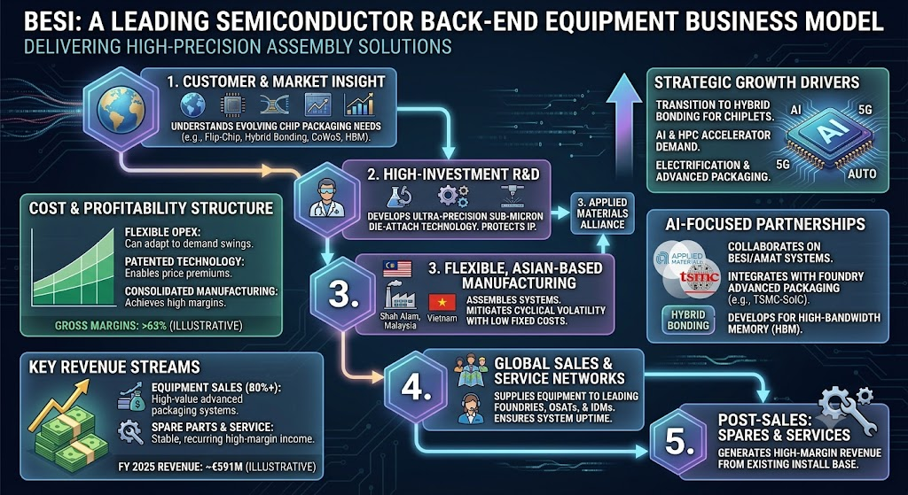
Besi generates revenue primarily through the development, production, and sale of specialized capital equipment used in the back-end assembly of semiconductor devices, complemented by high-margin spare parts and technical service contracts. The business model focuses on capturing the highest value-added segments of advanced packaging rather than competing in low-end, commodity wire-bonding.
Revenue Composition and Profit Mechanics
Besi organizes its core product lines around Die Attach systems (which generated approximately 80% of total revenue in fiscal 2025), Packaging systems (molding, trim, and form), and Plating equipment (the latter two contributing the remaining 20%). For fiscal year 2025, Besi generated €591.3 million in revenue and achieved a net income of €131.6 million. Its monetization model commands industry-leading gross margins—recording 63.3% in FY 2025 and 63.9% in Q4 2025—driven by patented placement accuracy down to sub-100 nanometers. While standard die bonders command unit selling prices in the range of hundreds of thousands of dollars, flagship hybrid bonding cluster tools carry average selling prices (ASPs) ranging between €1.5 million and €2.5 million per module, and complete multi-module systems can exceed €5 million to €8 million depending on automation and cleanroom specifications.
Strategic Growth Model
Besi operates a low fixed-cost manufacturing model where over 70% of production labor and assembly is based in Shah Alam (Malaysia) and its production facility in Vietnam, while high-value IP development remains concentrated in Europe. This structure allows the company to absorb 30% to 50% swings in cyclical semiconductor orders without collapsing into operating losses. Besi’s mid-term strategic model targets annual revenues of €1.7 billion to €2.2 billion with operating margins reaching 45% to 55%, underpinned by the industry transition from conventional solder-based microbumps (such as standard flip-chip and basic thermo-compression bonding) to direct copper-to-copper hybrid bonding.
Business Model Information Sources
- https://www.besi.com/investor-relations/press-releases/details/be-semiconductor-industries-nv-announces-q4-25-and-full-year-2025-results/
- https://quartr.com/companies/be-semiconductor-industries-n-v_4102
- https://www.besi.com/investor-relations/financial-reports/
Artificial Intelligence Strategy and Partnerships
Besi’s artificial intelligence strategy centers on providing the primary physical assembly infrastructure required to build high-performance AI processors, memory stacks, and optical networking components. As AI graphics processing units (GPUs) and application-specific integrated circuits (ASICs) hit physical reticle size limits, chipmakers rely on heterogeneous chiplet architectures that combine compute dies, high-bandwidth memory (HBM), and co-packaged optics (CPO). Besi targets this transition directly through its ultra-precision hybrid bonding and 2.5D/3D advanced packaging platforms.
R&D Budget Allocation
To maintain technological differentiation, Besi has doubled its annualized R&D investments since 2020. Research and development expenditure has expanded to exceed €60 million annually (representing 10% to 12% of total revenue depending on cyclical swings), with internal capital allocations tilted predominantly toward sub-100nm hybrid bonding accuracy, fluxless thermo-compression bonding (TCB), and automated particle-free wafer handling systems.
Strategic Industry Partnerships
- Applied Materials: In October 2020, Besi established a joint development initiative with Applied Materials to build unified die-based hybrid bonding equipment suites. This alliance integrates Applied Materials’ front-end deposition, chemical-mechanical planarization (CMP), etching, and surface-cleaning technologies with Besi’s high-speed, sub-micron placement tools. Demonstrating the long-term depth of the collaboration, Applied Materials acquired a 9% equity stake in Besi in April 2025.
- Foundry and OSAT Integration: Besi actively collaborates with Taiwan Semiconductor Manufacturing Company (TSMC) on integrating hybrid bonding into architectures such as TSMC-SoIC (System on Integrated Chips), as well as supporting advanced 2.5D substrate assembly (CoWoS). Besi’s customer roster has grown to 21 verified customers utilizing or qualifying its hybrid bonding platforms across logic, memory, and photonics applications.
- Memory and Photonics Collaborations: Besi collaborates with memory suppliers (such as Micron and SK Hynix) to transition future generations of HBM (specifically HBM4 and HBM4E) from microbump micro-reflow to hybrid bonding to mitigate thermal resistance and vertical height limitations. Additionally, Besi has partnered with data communications developers to adapt its 8800 Ultra platform for optical transceiver and co-packaged optics (CPO) assembly, addressing bandwidth bottlenecks inside AI hyperscale clusters.
Back to BE Semiconductor