The history of ASM International(ASMI) spans over half a century and can be categorized into four major key stages:
1. Foundation and Early Expansion(1968–1980s)
Founded in the Netherlands in 1968 by Arthur del Prado, the company started as a semiconductor materials distributor before developing its own manufacturing equipment. During the 1980s, it expanded globally, establishing backend packaging operations in Asia and listing on NASDAQ.
2. Strategic Investments and Giant Incubation(1980s–1990s)
During this era, ASMI founded and nurtured two companies that would become critical to the global tech ecosystem:
- ASML: Jointly founded in 1984 with Philips to develop lithography systems, later spun off independently in the 1990s.
- ASMPT: Developed backend packaging equipment in Asia, eventually growing into a worldwide leader in packaging systems.
3. The ALD Bet and Technical Pivot(1990s–2010s)
In 1999, ASMI acquired Microchemistry in Finland, securing key Atomic Layer Deposition(ALD) patents. Although ALD was initially dismissed as too slow, ASMI sustained heavy R&D. As silicon scaling hit physical limits, ALD became indispensable for High-k Metal Gate(HKMG) and FinFET architectures.
4. Pure-Play Focus and Advanced Node Leadership(2010s–Present)
ASMI gradually divested its stake in ASMPT to focus exclusively on front-end wafer fabrication equipment. Driven by the industry transition to Gate-All-Around(GAA) and 3D NAND architectures, demand for precise film deposition skyrocketed, cementing ASMI’s dominant market share of over 50% in ALD.
Source: ASM History and Milestones
Business Model
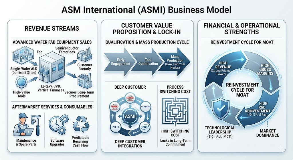
ASM International(ASMI) operates a high-barrier semiconductor capital equipment business model, generating revenue primarily through the development and sales of advanced front-end wafer fabrication equipment.
- Equipment Sales & Lock-in Effect: Core revenue is driven by sales of high-value thin-film deposition tools(ALD, Epitaxy, Vertical Furnaces). Because fab process switching costs are extremely high, once ASMI’s tools pass qualification and enter mass production with key customers(TSMC, Samsung, Intel), it secures multi-year tool procurement and recurring orders.
- Aftermarket Services & Consumables: As its global installed base expands, ASMI generates predictable, recurring cash flow from spare parts, maintenance services, and software upgrades, helping buffer semiconductor market cyclicality.
- High R&D Reinvestment & Margin Expansion: ASMI reinvests 10%–15% of annual revenue into R&D to preserve its technological moat. Leveraging its dominant market share(over 50%) in ALD, the company maintains strong pricing power and high gross margins.
Growth Strategy
ASMI’s strategy centers on fortifying its specialized moat and capturing upcoming architecture inflections:
- Pure-Play Focus: Unlike broad-portfolio competitors like Applied Materials or Tokyo Electron, ASMI executes a highly focused strategy, concentrating resources on thin-film deposition, particularly high-margin single-wafer ALD.
- Capitalizing on Architecture Inflections:
- Logic/Foundry: Capturing the transition to Gate-All-Around(GAA) and sub-2nm nodes, where atomic-level precision significantly increases ALD step intensity per wafer.
- Memory: Expanding deposition tool penetration in high-layer 3D NAND and HBM/DRAM scaling.
- Second Growth Engine(Epitaxy & SiC): Scaling its Epitaxy(Epi) business alongside ALD, while expanding into silicon carbide(SiC) tools for power electronics to diversify revenue streams.
- Co-Optimization with Key Customers: Engaging in joint development programs with top-tier semiconductor manufacturers early in their technology roadmaps, ensuring tool specifications align directly with future volume production requirements and blocking competitor entry.
Source: ASM Strategy & Investor Relations
AI Positioning & Strategy
ASM International plays a critical upstream role in the AI hardware ecosystem by providing precise thin-film deposition tools that enhance logic and memory chip performance:
- Logic Scaling(GAA & Sub-2nm): AI server processors(GPUs, ASICs) are transitioning to Gate-All-Around(GAA) architectures. This switch substantially increases the required intensity and step count of Atomic Layer Deposition(ALD).
- High Bandwidth Memory(HBM & DRAM): High-performance AI workloads rely on HBM and advanced DRAM. ASMI’s ALD and Epitaxy technologies are extensively applied to High-k Metal Gate(HKMG) structures and high-aspect-ratio memory features.
- Advanced Packaging & 3D Integration: Through targeted acquisitions(such as Axus Technology), ASMI has expanded its footprint into Chemical Mechanical Planarization(CMP) and advanced packaging/3D integration to support heterogeneous AI chip designs.
Partners & Key Customers
ASMI maintains deep co-development relationships and long-term supplier partnerships with the world’s leading foundries and memory makers:
- TSMC: Key supplier of ALD and Epitaxy tools for advanced logic manufacturing, specifically for N2/2nm and future GAA nodes.
- Samsung Electronics: Equipment supplier across advanced foundry nodes(SF3/GAA) and high-density memory lines.
- Intel: Deposition equipment provider supporting Intel 18A and advanced silicon nodes for AI chips.
- SK Hynix & Micron: Primary deposition vendor supporting volume production of HBM and next-generation DRAM architectures.
Budgets & Capital Allocation
- R&D Reinvestment: Consistently allocates 10%–15% of annual revenues to R&D, prioritizing single-wafer ALD, GAA tools, and advanced Epitaxy modules for AI-class chips.
- Capital Expenditures & Expansion: Investing hundreds of millions of euros into global facilities, including the expansion of its Dongtan R&D/manufacturing center in South Korea for AI memory tools and the expansion of its Scottsdale/Phoenix headquarters in Arizona.
- Strategic M&A: Utilizing a robust net-cash position(exceeding €1 billion) to execute tuck-in acquisitions—such as its acquisition of Axus Technology—to secure critical positions in advanced packaging and compound semiconductors.
Sources:
Back to ASM