
Corporate History
- Founding and Early Precision Instruments(1954–1970s): Founded in 1954 as Takeda Riken Industry Co., Ltd., the company initially specialized in electronic measuring instruments and precision counting equipment, later developing Japan’s first electronic digital voltmeter.
- Transition to Semiconductor Testing and Global Expansion(1970s–1990s): Recognizing the rise of integrated circuits, the company pivoted into automated test equipment, introducing the 100MHz VLSI test system in 1979. It rebranded as Advantest Corporation in 1985 and listed on the Tokyo Stock Exchange to expand international subsidiaries across North America, Europe, and Asia.
- Consolidation and Strategic M&A(2000s–2010s): Advantest listed on the New York Stock Exchange in 2001(later delisted in 2016 to optimize capital allocation). A transformative milestone came in 2011 with the acquisition of US-based Verigy for approximately $1.1 billion, which unified the V93000 platform and cemented Advantest’s leadership in SoC logic testing.
- The AI and Advanced Packaging Supercycle(2020s–Present): Entering the post-pandemic era, Advantest established a near-monopolistic position in testing AI accelerators and HBM stack architectures. In response to surging demand, the company launched its updated “Grand Design” and third Mid-Term Management Plan(MTP3) to aggressively scale manufacturing and software ecosystems.
Business Model and Growth Strategy
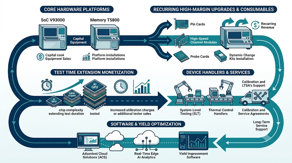
Advantest operates a platform-plus-service business model where the monetization mechanism centers on high-margin modular hardware platforms, high-frequency test consumables, and recurring post-sales engineering support:
- Hardware Platform & Upgrade Modules: Advantest sells foundational automated test frames—principally the flagship V93000(SoC) and T5800/T5500(Memory) series. Because these platforms feature modular card cages, customers do not discard machines when moving between chip generations; they buy incremental pin cards, power supplies, and high-frequency digital channels at substantial gross margins(often exceeding 60% during peak mix cycles).
- Test Time Extension Monetization: Chip complexity directly drives Advantest’s top line. As AI GPUs and HBM3E/HBM4 stacks transition to 2.5D/3D chiplet configurations, structural defects increase exponentially. Because thorough verification causes test times to lengthen two-to-threefold, chipmakers must order significantly more tester units simply to maintain identical unit throughput.
- Device Interfaces and Maintenance Services: The company captures high-margin recurring cash flows via probe cards, dynamic change kits, device handlers, calibration services, and long-term service agreements(LTSAs), insulating the balance sheet during chip market downturns.
- Financial Strategy Metrics: Under its updated MTP3 management plan, Advantest targets average annual sales of JPY 835–930 billion with operating profit margins sustained around 33–36% and Return on Invested Capital(ROIC) between 18–28%, allocating over JPY 600 billion in operating cash flows toward capacity expansion, R&D, and a minimum 50% cumulative shareholder return ratio.
Sources for Business Model
- https://www.advantest.com/document/en/investors/ir-library/annual/E_02_IAR2025.pdf
- https://www.advantest.com/document/en/investors/ir-library/investors-guide/Investors_Guide_2604E.pdf
- https://newsfile.futunn.com/public/NN-PersistNoticeAttachment/7781/20240625/JPX/20240625536222.PDF
- https://www.investing.com/news/transcripts/earnings-call-transcript-advantests-record-q1-2025-sales-and-growth-strategy-93CH-4325840
AI Strategy, Budget, and Ecosystem Partnerships
Advantest has repositioned its core strategic focus to address the multi-die complexity, thermal extremes, and massive pin-count requirements of generative AI hardware:
- Product Development for HBM and AI Silicon: Advantest dominates testing for HBM stacks(estimated at over 60% market share) and advanced GPU/ASIC accelerators. Its solutions target Known Good Die(KGD) testing at wafer probe, high-speed interface characterization, and high-power system-level testing(SLT) capable of dissipating thermal design loads exceeding 1,000 watts during test cycles.
- Advantest Cloud Solutions(ACS): Advantest expanded beyond raw measurement hardware into an open data platform called ACS. ACS applies real-time edge AI algorithms directly on the tester to analyze parametric data streams, detect outlier dies early in the fabrication flow, dynamically adjust testing routines, and directly improve wafer yields for advanced sub-3nm nodes.
- R&D Allocations and Capital Expenditure: Advantest invests approximately JPY 65–75 billion annually in research and development(accounting for 8–10% of revenue). In capital allocation, the company committed capital investments to expand manufacturing and integration capacity by over 70% to alleviate delivery lead-time constraints for next-generation AI platforms.
- Key Ecosystem Partners: Advantest maintains deep operational alignment across all nodes of the leading-edge AI compute ecosystem:
- Fabless AI Leaders: Tight co-development programs with Nvidia and AMD, embedding Advantest test configurations as the reference standard for frontier AI GPUs.
- Foundry & Advanced Packaging: Close integration within TSMC’s OIP(Open Innovation Platform) 3DFabric alliance, coordinating test standards across CoWoS(Chip-on-Wafer-on-Substrate) and SoIC architectures.
- Memory Manufacturers: Primary verification supplier for SK Hynix, Samsung Electronics, and Micron Technology across their HBM3E and HBM4 roadmaps.
Back to Advantest