Hyundai Electronics Era (1983-1998)
SK Hynix originated as Hyundai Electronics in 1983. During this period, South Korea aggressively entered the semiconductor market. By 1985, the company successfully developed 256K NMOS DRAM. The focus was on rapid technological catch-up and massive capacity expansion to compete with Japanese and American chipmakers.
Core Technology: 256K NMOS DRAM, 64M/128M SDRAM.
Core Strategy: Catch-up and Expansion. Leveraged government support and Hyundai Group capital to build massive production capacity, rapidly closing the gap with US and Japanese leaders.
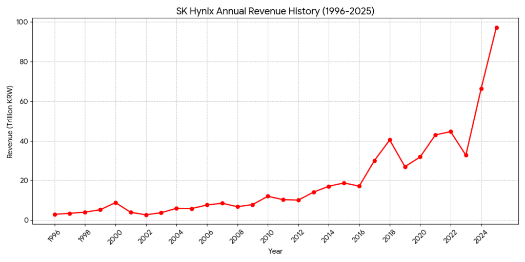
Revenue Level: Annual average 1T to 5T KRW. High growth driven by capacity, but focused on low-margin commodity DRAM.
Crisis and Independence (1999-2011)
Following the 1997 Asian Financial Crisis, Hyundai Electronics merged with LG Semiconductor in 1999. In 2001, it spun off from the Hyundai Group and was renamed Hynix. This was the most difficult chapter in its history, marked by heavy debt, DRAM price crashes, and trade sanctions from the US and EU. Despite being managed by creditor banks, Hynix survived through extreme cost-cutting and persistent R&D.
Core Technology: 80nm packaging technology, 2Gb DDR3, early-stage 50nm-class DRAM.
Core Strategy: Survival and Efficiency. Under creditor management and heavy debt, the company pivoted to “high-efficiency R&D,” maintaining technical relevance through extreme cost-cutting and yield optimization.
Revenue Level: Annual average 9T to 12T KRW. Highly volatile revenue due to memory market cycles and financial instability.
SK Group Acquisition (2012-2022)
In 2012, SK Telecom acquired a controlling stake, and the company became SK Hynix. The infusion of capital from SK Group allowed the company to pivot from survival to aggressive investment. Key milestones included:
- 2013: Mass production of 16nm NAND Flash.
- 2020: Announcement of the $9 billion acquisition of Intel’s NAND and storage business (Solidigm), significantly boosting its enterprise SSD market share.
Core Technology: 16nm NAND, 1anm DRAM, early HBM development.
Core Strategy: Capital Investment and M&A. With SK Group’s financial backing, the company shifted from survival to aggressive expansion, culminating in the $9B acquisition of Intel’s NAND business (Solidigm) to balance its portfolio.
Revenue Level: Annual average 18T to 45T KRW. Revenue doubled as the company captured the surge in server and smartphone demand.
AI Leadership and HBM Dominance (2023-Present)
With the explosion of Generative AI, SK Hynix has emerged as the global leader in High Bandwidth Memory (HBM). By securing a primary supplier position for NVIDIA’s AI GPUs, the company shifted from a market follower to a trendsetter. It was the first to mass-produce HBM3 and HBM3E, giving it a significant competitive edge in the high-end memory market.
Core Technology: HBM3/HBM3E (World-first mass production), 321-layer NAND, 1cnm DRAM.
Core Strategy: Profit-First and AI Specialization. Focused on the NVIDIA supply chain and reallocated resources from generic DRAM to high-margin AI memory, transforming from a market follower into an industry trendsetter.
Revenue Level: 66.2T KRW (2024), 97.1T KRW (2025 estimate). Achieved record-breaking revenue and margins driven by the AI super-cycle.
In 2026, SK Hynix has solidified its transition from a market follower to a specialized high-margin leader. The competitive landscape is defined by its dominance in AI-specific memory and its strategic alliance with the logic foundry ecosystem.
1. Market Share & Profitability (2026 Status)
SK Hynix has achieved a historic milestone by outperforming Samsung Electronics in annual operating profit for the 2025 fiscal year, driven by its 62% market share in the High Bandwidth Memory (HBM) segment.
- SK Hynix: Controls ~62% of the HBM market. Its revenue is projected to reach 162 trillion KRW in 2026.
- Micron: Following a “technology-first” strategy, Micron has overtaken Samsung to become the second-largest HBM supplier with a ~21% share.
- Samsung: Currently in a “counter-offensive” phase with a ~17% HBM share, focusing on regaining ground through its massive R&D resources and its integrated 4nm/2nm foundry services.
2. Strategic “Twin Engine” Analysis
SK Hynix’s 2026 strategy relies on balancing high-end AI components with tight supply management in traditional markets.
- The HBM Engine: The company has already sold out its HBM capacity for the entirety of 2026. It is the first to mass-produce 16-layer HBM4, achieving data rates of 10 Gbps and 40% better power efficiency.
- The Commodity Engine: By reallocating DRAM production lines to HBM, SK Hynix has intentionally tightened the supply of standard DDR5. This “scarcity strategy” is expected to drive conventional DRAM prices up by 60% in early 2026, boosting margins across its entire portfolio.
3. Key Technological Battlegrounds
| Feature | SK Hynix (The Leader) | Samsung (The Integrated Rival) | Micron (The Efficiency Challenger) |
| HBM4 Approach | Alliance Model: Partnering with TSMC to use 12nm/5nm logic for the base die. | Turnkey Model: Integrated memory + Samsung Foundry + Advanced Packaging. | In-house Focus: High-speed 11 Gbps samples using proprietary 1β nodes. |
| Packaging | MR-MUF: Proprietary tech allowing thinner wafers (30 um) for 16-layer stacks. | TC-NCF: Refining non-conductive film to match MR-MUF thermal performance. | Hybrid Bonding: Investing heavily in next-gen bonding for HBM4E. |
| Enterprise SSD | Leading with Solidigm 60TB/120TB QLC drives for AI training data. | Shifting focus to high-capacity V-NAND to recover enterprise market share. | Emerging as a strong competitor in high-speed NVMe for AI edge devices. |
4. SWOT Analysis (2026 Perspective)
- Strengths:
- NVIDIA Synergy: Deep integration into the “Blackwell” and “Rubin” GPU roadmaps.
- Financial Health: Upgraded to BBB+ by S&P Global due to record cash flows and a debt-to-equity ratio below 20%.
- Weaknesses:
- High Concentration: Extreme reliance on AI-related demand; a “cooling” in AI CAPEX would disproportionately hurt Hynix compared to the more diversified Samsung.
- Opportunities:
- HBM4 Customization: The move toward “Custom HBM” allows Hynix to lock in long-term contracts with hyperscalers like Microsoft and Google.
- Threats:
- The “AI Premium” Erosion: Analysts expect HBM average selling prices (ASP) to potentially drop by 7-10% as Samsung and Micron ramp up HBM4 supply.
Source:
- History & Milestones: SK hynix – History
- Corporate Timeline (Hyundai to SK): Zippia – SK Hynix History: Founding, Timeline, and Milestones
- 2025 Financial Performance: SK hynix Newsroom – SK hynix Posts Record Annual Financial Results in 2025
- 2024 Financial Performance: Taiwan News – SK hynix Announces FY25 Financial Results (Includes FY24 data)
- HBM Market Share & Analysis: TrendForce – How AI Growth Will Drive HBM Demand Beyond 2025
- DRAM & NAND Competitive Dynamics: The Korea Herald – NAND prices surge as Korean memory giants prioritize HBM
- TSMC Partnership (HBM4): Mobile World Live – SK Hynix, TSMC team on next-gen memory
- HBM4 & CXL Collaboration: DIGITIMES Asia – SK Hynix deepens strategic partnership with TSMC
- Intel NAND Acquisition (Solidigm): SK Group – SK Hynix Completes First Phase in its Acquisition of Intel’s NAND Flash Business
- Acquisition Completion Details: moomoo – SK hynix has completed the acquisition of Intel’s NAND business
Back to SK Hynix page