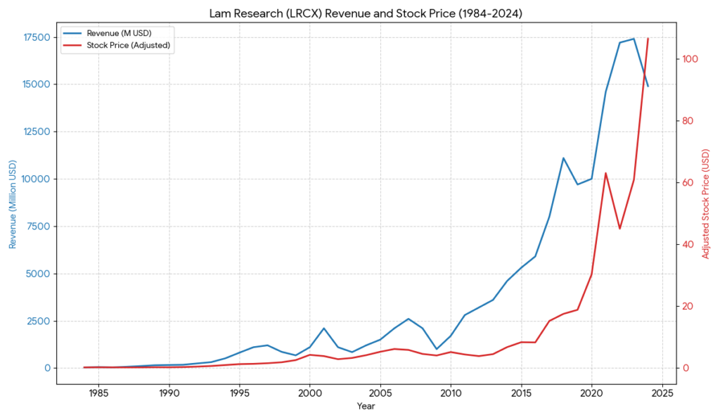
1. Foundation and Etch Leadership (1980–1989)
This era established Lam Research as a pioneer in the plasma etch market.
- 1980: Founded by David K. Lam in Santa Clara, California, to address the need for advanced plasma etching in semiconductor manufacturing.
- 1981: Introduced the AutoEtch 400, the industry’s first fully automated plasma etching system, replacing manual wet-etching processes.
- 1984: Completed its Initial Public Offering (IPO) on the NASDAQ under the ticker LRCX.
- 1987: Relocated headquarters to Fremont, California, and launched the Rainbow etch system.
2. Global Expansion and Deposition Entry (1990–2000)
Lam expanded its global footprint and diversified its technology portfolio beyond etching.
- 1992: Launched Transformer Coupled Plasma (TCP) technology, which set a new industry standard for high-performance etching.
- 1993: Entered the deposition market with the release of the Altus Tungsten Chemical Vapor Deposition (CVD) system.
- 1997: Acquired OnTrak Systems, marking Lam’s entry into the wafer cleaning and CMP (Chemical Mechanical Polishing) market.
3. Strategic Consolidation and Transformation (2001–2012)
This period saw Lam transform into a comprehensive equipment supplier through massive acquisitions.
- 2008: Acquired SEZ Group, strengthening its position in the single-wafer cleaning market.
- 2012: Merged with Novellus Systems in a 3.3 billion USD deal. This was a pivotal moment, as it brought industry-leading Chemical Vapor Deposition (CVD) and Electroplating technologies under Lam’s roof, allowing it to compete directly with Applied Materials across the entire fabrication line.
4. The Era of AI and Advanced Packaging (2013–Present)
Lam is currently focused on enabling sub-3nm nodes, 3D NAND stacking, and advanced packaging for AI chips.
- 2020: Celebrated its 40th anniversary and launched the Sense.i etch platform, which utilizes AI and big data analytics to improve tool performance and reliability.
- 2022: Acquired SEMSYSCO, enhancing its capabilities in heterogeneous integration and Chiplet packaging.
- Current Status: Lam Research remains the dominant leader in 3D NAND manufacturing equipment and is a critical partner for logic manufacturers using EUV (Extreme Ultraviolet) lithography with its dry resist technology.
As of 2026, the technical battleground has shifted to three critical frontiers:
1. The Etch War: Lam Cryo 3.0 vs. TEL Cryogenic
In the 3D NAND race toward 400+ layers, the “memory hole” etch is the single most difficult step in semiconductor manufacturing.
- Lam’s Technical Moat (Cryo 3.0): Lam’s latest cryogenic etching uses extremely low temperatures and proprietary pulsed-plasma chemistry. It enables high-speed etching of deep channels while maintaining a perfectly vertical profile.
- The Competitive Edge: Lam has integrated its Sense.i platform (AI-driven sensors) into the etch chamber. This allows for real-time adjustments to plasma uniformity, achieving a “wafer-to-wafer” consistency that Tokyo Electron (TEL) still struggles to match at the 300-layer threshold.
- TEL’s Threat: TEL’s high-speed cryogenic etch is faster in terms of raw throughput, but Lam leads in Yield (Selectivity)—ensuring that the mask isn’t destroyed before the hole reaches the bottom.
2. The Lithography Expansion: Dry Resist vs. Wet Resist
This is Lam’s strategic “flanking maneuver” against the traditional lithography ecosystem.
- The Problem: Traditional Wet Resist (supported by TEL’s tracks) faces “pattern collapse” at 2nm and below because the liquid tension pulls the tiny features over.
- Lam’s Innovation (Aether Platform): Lam is the only company offering Dry Resist technology for EUV. By using vapor-phase deposition instead of spinning liquid chemicals, Lam creates a much denser, more uniform film.
- Technical Superiority: * Resolution: Dry resist allows for much higher contrast, which is essential for High-NA EUV.
- Sustainability: It uses 5x to 10x less raw material than wet chemistry, significantly lowering the “Cost per Exposure” for giants like TSMC and Intel.
3. Logic Leadership: Backside Power & Molybdenum (Mo)
As logic chips move to 2nm (GAA architecture), the wiring (interconnects) becomes a bottleneck due to high electrical resistance.
- The Molybdenum Transition: Lam is leading the charge to replace Tungsten with Molybdenum (Mo) for the first metal layers. Lam’s ALTUS ALD (Atomic Layer Deposition) systems can deposit Mo at near-zero resistivity at the atomic scale.
- Backside Power Delivery (BSPDN): This is the most significant architectural change in 30 years. It requires flipping the wafer and etching deep vias from the back.
- LRCX vs. AMAT: While AMAT excels in the chemical-mechanical polishing (CMP) needed for this, Lam owns the High-Selectivity Etch required to stop exactly at the transistor layer without damaging the device.
Technical Leadership Matrix (2026 Forecast)
| Domain | Lam Research (LRCX) | Applied Materials (AMAT) | Tokyo Electron (TEL) |
| 3D NAND Etching | Dominant (Cryo 3.0) | Moderate | Strong (Challenger) |
| EUV Dry Resist | Monopoly | N/A | N/A (Supports Wet) |
| ALD (Atomic Layer) | Leader (Metal ALD) | Strong (CVD/PVD) | Moderate |
| Advanced Packaging | Leader (TSV/Electroplate) | Strong | Moderate |
Strategic Conclusion
Lam Research has successfully pivoted from being “the memory guy” to becoming the “enabler of 3D logic.” By owning the Dry Resist and High-Aspect-Ratio Etch niches, Lam makes itself indispensable for the 2nm/1.4nm nodes and HBM3e/HBM4 production.
Source:
- https://www.lamresearch.com/company/history/
- https://en.wikipedia.org/wiki/Lam_Research
- https://www.lamresearch.com/products/our-solutions/aether/
- https://www.lamresearch.com/products/our-solutions/cryogenic-etching/
- https://www.semi.org/en/semi-press-release/lam-research-receives-2025-semi-award-for-north-america
- https://www.macrotrends.net/stocks/charts/LRCX/lam-research/revenue
- https://www.forbes.com/companies/lam-research/
- https://www.morningstar.com/stocks/xnas/lrcx/quote
- https://www.mordorintelligence.com/industry-reports/semiconductor-equipment-market
Back to Lam Research page