Market Position and Market Share
Tokyo Electron Limited (TEL) ranks as the 4th largest semiconductor manufacturing equipment (WFE – Wafer Fab Equipment) vendor globally by revenue, behind ASML, Applied Materials (AMAT), and Lam Research. In the overall global WFE market, TEL holds an estimated 11% to 12% total value share.
TEL holds near-monopolistic and leading market shares across several core process segments:
- Coater/Developer (Track Systems): TEL commands roughly 89% to 91% global market share, and effectively holds a 100% monopoly in track systems integrated with Extreme Ultraviolet (EUV) lithography scanners alongside ASML.
- Etch Systems (Dry Plasma Etch): TEL ranks 2nd globally with approximately 25% to 29% market share, competing directly with Lam Research (the category leader) and Applied Materials.
- Thermal Processing / Oxidation / Diffusion Furnaces: TEL holds the #1 or #2 global position with approximately 45% to 50% market share.
- Single-Wafer Deposition & ALD (Atomic Layer Deposition): TEL captures roughly 30% to 35% in targeted ALD niches, ranking behind ASM International and Applied Materials.
- Wafer Probers: Dominates the front-end testing interface with over 35% to 40% global share.
Supply Chain Analysis and Key Suppliers
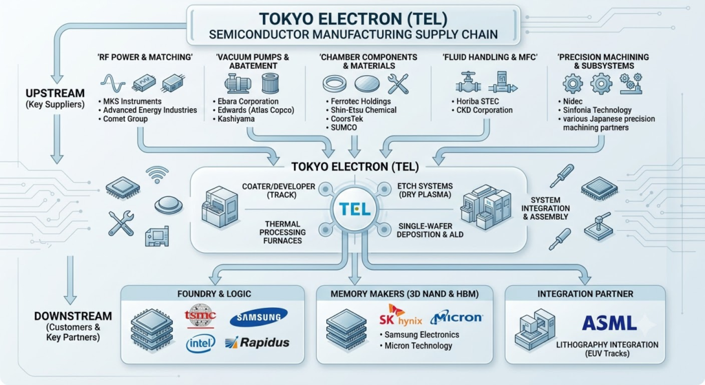
TEL sits in the mid-stream of the broader semiconductor ecosystem, supplying equipment to front-end fabrication plants (fabs). Its operational model relies on high-mix, low-volume assembly, where precision subsystem manufacturing is outsourced to specialized tier-1 and tier-2 component vendors.
Upstream (Component, Subsystem, and Raw Material Suppliers)
TEL procures specialized sub-assemblies, precision chambers, motion control stages, and radio frequency (RF) generators. Key suppliers include:
- RF Power Generators & Matching Networks:MKS Instruments (MKSI) and Advanced Energy Industries (AEIS). These provide the critical RF power delivery required to sustain stable plasma in TEL’s etch and PECVD chambers.
- Vacuum Pumps & Abatement Systems: Ebara Corporation, Edwards Vacuum (Atlas Copco), and Kashiyama. Dry vacuum pumps and gas abatement scrubbers are essential for maintaining high-vacuum chamber integrity and neutralizing toxic process effluents.
- Precision Ceramics, Quartz, and Silicon Electrodes: Ferrotec Holdings, Shin-Etsu Chemical, and CoorsTek. These provide consumable and non-consumable chamber components (e.g., quartz rings, ceramic electrostatic chucks, and showerheads) designed to withstand corrosive halogen plasma environments.
- Fluid Handling, Valves, and Mass Flow Controllers (MFC): Horiba STEC and CKD Corporation provide ultra-clean chemical/gas flow control modules for atomic-scale gas dosing.
- Contract Machining and Module Assembly: Japanese precision machining partners such as Ferrotec and domestic tier-2 machine shops handle chamber casting and surface anodization.
Downstream (Customers and Integration Ecosystem)
TEL supplies the world’s leading semiconductor manufacturers across three primary pillars:
- Foundry & Logic: TSMC, Samsung Electronics Foundry, and Intel. TEL’s coater/developer tracks form an inseparable inline module paired with ASML scanners in advanced sub-3nm nodes, while its cryogenic etch systems target GAA (Gate-All-Around) nanosheet structuring.
- Memory Makers: Micron Technology, SK Hynix, and Samsung Electronics. Etching and thermal processing systems are heavily deployed in high-aspect-ratio (HAR) contact hole etching for >200-layer 3D NAND and TSV (Through-Silicon Via) processing for High Bandwidth Memory (HBM).
- Lithography Integration Partner:ASML. While not a direct commercial buyer, ASML operates as a vital co-development ecosystem partner; TEL’s track hardware physically links and coordinates wafer staging for ASML EUV systems.
Competitor Analysis: Technology and Financial Comparison
TEL faces direct competition primarily from US and European equipment peers: Applied Materials (AMAT), Lam Research (LRCX), and to a specialized extent, ASML and KLA.
Technological Comparison
- Track / Lithography Interfacing: TEL maintains an almost unassailable moat. Applied Materials exited this space decades ago, leaving TEL virtually unchallenged in advanced EUV tracks.
- Etching Technology: Lam Research remains the benchmark in high-aspect-ratio dielectric etch (critical for 3D NAND channels). However, TEL has challenged Lam’s dominance by introducing cryogenic dielectric etch technology, which utilizes sub-zero temperatures (e.g., -70°C) to accelerate etch rates and etch 10-micrometer-deep holes with vertical profiles at significantly lower power consumption. In conductor/metal etch, Applied Materials and TEL compete closely.
- Deposition & ALD:Applied Materials holds the broadest portfolio in CVD, PVD, and epitaxial deposition. ASM International (ASMI) leads in single-wafer ALD for logic high-k metal gates. TEL competes primarily via batch ALD and semi-critical chemical vapor deposition where uniform thermal profile furnaces are required.
- Process Breadth: Unlike Lam Research (heavily etch/deposition-centric) or ASML (pure-play lithography), TEL possesses equipment across four sequential manufacturing steps (clean, coat/develop, etch, and thermal deposition), allowing it to optimize integrated defect management across the entire patterning loop.
Financial Comparison
- Revenue Base:TEL generates roughly ¥2.4T to ¥2.6T (~$16B to $18B USD), placing it comparable in scale to Lam Research (~$17B to $21B USD), but below Applied Materials (~$27B to $28B USD) and ASML (~$30B to $35B USD).
- Operating Margins: TEL typically delivers operating margins in the 26% to 30% range. In comparison:
- KLA leads the broader peer group with operating margins of ~38% due to high-margin software/inspection IP.
- ASML operates at ~34% to 35% margins driven by its EUV pricing power.
- Lam Research achieves ~30% to 32% operating margins.
- Applied Materials posts ~28% to 29% operating margins.
- Capital Return & R&D Commitment:TEL maintains high return on equity (ROE > 25%–30%) and reinvests heavily in technology, committing ¥1.5 trillion in cumulative R&D investments across FY2025–FY2029. Lam Research and AMAT allocate greater portions of free cash flow to aggressive share buyback programs, whereas TEL balances dividend payout targets (~50%) with substantial cash reserves to buffer semiconductor cyclicality.
- Geographic & China Exposure: TEL, Lam, and AMAT have all experienced elevated revenue exposure to mainland China (often 35% to 45%+ of total quarterly revenues during recent trailing periods) driven by legacy node build-outs. However, TEL faces differing geopolitical trade constraints compared to US vendors, navigating Japanese export control frameworks while remaining restricted from exporting leading-edge GAA/EUV-related equipment to non-compliant entities.
Sources
- https://www.tel.com/corporatesummary/
- https://www.tel.com/sustainability/management-foundation/supply-chain-management/index.html
- https://sharedresearch.jp/en/companies/8035
- https://www.techinsights.com/blog/wFE-market-share
- https://fffinstill.com/blog/semiconductor-equipment-asml-lrcx-amat-klac-compared
- https://www.lovechip.com/blog/top-10-semiconductor-equipment-manufacturers-in-2024-shaping-the-future-of-chipmaking
- https://www.mordorintelligence.com/industry-reports/semiconductor-etch-equipment-market
Back to Tokyo Electron