Company History TradingKey
Foundation and Toshiba Memory Era(1987–2017)
- 1987: Toshiba engineer Dr. Fujio Masuoka invents NAND flash memory, establishing the technical foundation for solid-state storage. Umbrex
- 2000–2015: Formed a long-term manufacturing joint venture with SanDisk(later acquired by Western Digital) to co-invest in the Yokkaichi fab complex in Mie Prefecture.
- 2017: Toshiba Corporation, facing bankruptcy risks from catastrophic nuclear plant construction losses at Westinghouse, decided to spin off its crown-jewel memory chip unit into Toshiba Memory Corporation.
Bain Capital Consortium Buyout and Rebranding(2018–2023)
- 2018: Toshiba Memory was acquired for approximately ¥2 trillion by a Bain Capital-led consortium(including SK Hynix, Apple, Dell, and Kingston Technology), while Toshiba retained a minority stake.
- 2019: The company rebranded globally as Kioxia Holdings Corporation, combining the Japanese word kioku(memory) and the Greek word axia(value).
- 2020–2023: Kioxia navigated market downturns, aborted several planned Tokyo IPO attempts due to market turbulence, and engaged in prolonged, complex merger negotiations with Western Digital’s flash division, which ultimately stalled due to SK Hynix’s opposition. Umbrex
Public Listing and AI-Driven Growth(2024–Present)
- December 2024: Kioxia completed its long-awaited initial public offering(IPO) on the Tokyo Stock Exchange(Prime Market, TYO: 285A). TradingKey
- 2025–2026: Capitalized on structural NAND supply shortages and explosive data center capacity demands spurred by generative AI inference, successfully commercializing next-generation BiCS 3D NAND architectures and returning to record profitability. StockAnalysis.com+ 1
Business Model and Strategic Execution
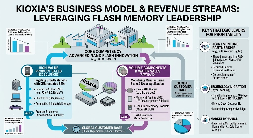
Kioxia operates a high-fixed-cost, volume- and yield-driven semiconductor business model. The company monetizes memory through two primary operational channels:
Umbrex
- Raw NAND Flash Wafer and Component Sales: Standard NAND flash sold directly or via joint venture off-takes to module makers, mobile device OEMs, and computing device integrators.
- Engineered Storage Solutions(Enterprise and Client SSDs): High-margin enterprise, cloud data center, and client SSDs integrated with in-house proprietary controllers and firmware, which deliver premium average selling prices(ASPs).
Profit Generation Mechanics and Operational Scale
- Joint Venture Cost-Sharing: Kioxia shares cleanroom construction, tooling, and wafer production costs at Yokkaichi and Kitakami with Western Digital/SanDisk, allowing it to achieve Samsung-equivalent manufacturing scale at roughly half the direct capital outlay.
- Layer Migration and Cost-Per-Bit Depletion: Profitability is dictated by reducing manufacturing cost per bit faster than memory ASP depreciation. In high-demand cycles, high fab utilization yields massive non-GAAP operating margin expansion.
- Financial Performance: For FY2025, Kioxia reported revenue of ¥2,337.6 billion(up from ¥1,706.5 billion in FY2024). Non-GAAP operating profit reached ¥876.2 billion, achieving an operating margin of 37%(compared to 27% in FY2024), driven by high-density enterprise SSD deployment and tighter supply discipline. キオクシアホールディングス株式会社
Sources for Business Model Information
- https://www.kioxia-holdings.com/en-jp/ir/earnings/highlights.html
- https://umbrex.com/resources/company-profiles/kioxia-holdings-corp/
- https://the-shashi.com/en/tse/285A/financials/
AI Strategic Initiatives, Budget, and Partnerships
Strategic Positioning in the AI Memory Stack While DRAM and HBM process active GPU computations, AI training clusters and real-time inference workloads face significant I/O bottlenecks when fetching massive datasets. Kioxia focuses on ultra-high-density, low-latency enterprise SSDs and CXL(Compute Express Link) memory tiers designed for large language model(LLM) inference servers and retrieval-augmented generation(RAG) pipelines.
Capital Expenditure and R&D Budget
- Multi-Year Capital Expenditure Program: Kioxia and its joint venture partner outlined a planned capital expenditure program exceeding ¥5 trillion(approximately $31.4 billion) over six years across Japanese production sites to support AI-driven infrastructure demand. Taipei Times
- Annual Allocation: Kioxia has allocated approximately ¥470 billion annually toward capital expenditures and approximately ¥230 billion annually toward dedicated R&D programs, targeting advanced layer-stacking techniques and high-speed controller interfaces. キオクシアホールディングス株式会社
- Fab Expansion: A dedicated ¥1.8 trillion allocation was directed to scale Fab 2(K2) at the Kitakami plant in Iwate Prefecture, configured specifically for advanced 218-layer and 10th-generation BiCS 3D flash production dedicated to enterprise AI workloads. Umbrex
Key Commercial and Ecosystem Partnerships
- Western Digital / SanDisk: Core joint venture partner for co-developing 3D NAND flash nodes(BiCS8 and BiCS10) and co-funding manufacturing fab capacity in Yokkaichi and Kitakami.
- Hyperscale Cloud Service Providers: Long-term multi-year supply and product validation agreements with major hyperscalers, including Microsoft Azure, Meta Platforms, and Alphabet, to integrate PCIe 5.0 and PCIe 6.0 enterprise SSDs directly into AI training clusters and inference data centers.
- Japanese Government Subsidies: The Japanese Ministry of Economy, Trade and Industry(METI) has granted hundreds of billions of yen in subsidies to Kioxia’s Yokkaichi and Kitakami facilities to maintain sovereign cutting-edge semiconductor manufacturing capacity in Japan.
Back to Kioxia