
Market Position and Market Share
BE Semiconductor Industries N.V.(Besi) is a leading global designer and manufacturer of semiconductor assembly and packaging equipment, with primary dominance in the advanced packaging and die attach segments.
- Overall Die Attach Market: Besi holds the #1 market position worldwide in high-precision die attach equipment, capturing an estimated 30% to 35% global market share in high-accuracy die bonding applications, competing closely with ASMPT in broader die attach tool categories. In the total semiconductor bonding market(comprising die bonders, wafer bonders, and hybrid bonders), Besi commands an estimated revenue share of roughly 9% to 13%.
- Advanced Packaging & Die-to-Wafer(D2W) Hybrid Bonding: Besi is the clear pioneer and market leader in ultra-fine pitch Die-to-Wafer hybrid bonding equipment, commanding an estimated market share exceeding 70% to 80% in high-volume manufacturing(HVM) hybrid bonding placements. Its flagship tooling, the 8800 Ultra and 8800 Cham hybridization series, achieves sub-100-nanometer to sub-200-nanometer placement accuracy, making Besi the dominant equipment vendor for next-generation AI accelerators, heterogeneous chiplet integration, and 3D stacked logic-on-logic architectures.
Supply Chain Analysis and Key Suppliers
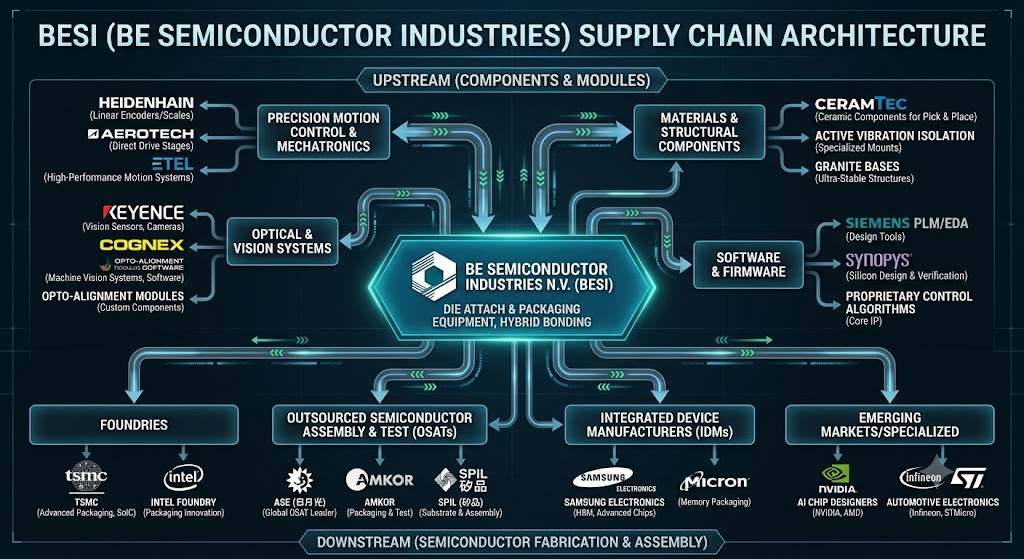
Besi operates an asset-light, modular assembly operational model, relying heavily on outsourced precision manufacturing while maintaining proprietary core motion-control algorithms, calibration firmware, and high-accuracy assembly in-house.
- Upstream Supply Chain:
- Precision Motion Control & Stages: Advanced die bonders require sub-micron precision positioning. Core inputs include high-frequency linear motors, optical linear encoders, and air-bearing motion stages sourced from specialized motion control vendors(such as Heidenhain, Aerotech, and ETEL).
- Optical & Vision Systems: Besi integrates high-resolution telecentric optical lenses, high-speed image processing cameras, and infrared/laser alignment sensors(often sourced from specialist machine-vision suppliers such as Keyence and Cognex, alongside proprietary optical calibration heads) to ensure sub-micron wafer-to-die alignment.
- Structural Base & Vibration Isolation: Machine frames utilize ultra-dense synthetic or natural granite bases and active pneumatic vibration-isolation mounts to dampen shop-floor acoustic and mechanical resonance during ultra-high-speed placement cycles.
- Manufacturing Footprint: Besi distributes fabrication across low-cost Asian production hubs and high-precision European centers. Core system development and initial precision calibration take place in Duiven(Netherlands), Radfeld(Austria), and Cham(Switzerland), while high-volume sub-assembly, frame manufacturing, and module integration are concentrated in Shah Alam(Malaysia) and Leshan(China).
- Downstream Supply Chain:
- Pure-Play Foundries: Tier-1 foundries(notably TSMC for its CoWoS, SoIC, and 3DFabric platforms) represent critical end-customers for leading-edge hybrid bonding and flip-chip attach systems.
- Integrated Device Manufacturers(IDMs): Leading IDMs such as Intel(for Foveros 3D packaging) and major memory manufacturers like Micron and SK Hynix utilize Besi’s high-precision placement solutions for high-density interconnects and memory stacking.
- Outsourced Semiconductor Assembly and Test(OSATs): OSAT giants including ASE Technology Holding, Amkor Technology, and JCET deploy Besi’s mainstream flip-chip, multi-module, and thermo-compression bonders for automotive, communication, and consumer electronics modules.
Competitor Analysis
Besi competes against distinct groups of equipment makers across standard back-end packaging and front-end/hybrid-bonding transitions.Its principal competitors include ASMPT, Kulicke & Soffa(K&S), EV Group(EVG), and Hanmi Semiconductor.
- Technical Comparison:
- Besi vs. ASMPT: ASMPT has a broader total portfolio spanning wire bonding, surface-mount technology(SMT), and die attach. While ASMPT has entered the hybrid bonding space with its LithoBolt and FireBird systems, Besi maintains a multi-year head start in Die-to-Wafer(D2W) hybrid bonding precision(<100 nm to <200 nm accuracy), supported by its development partnership with Applied Materials. ASMPT dominates volume-driven packaging tools, whereas Besi leads in ultra-precision, high-end chiplet packaging.
- Besi vs. EV Group(EVG) & SUSS MicroTec: EVG and SUSS primarily dominate Wafer-to-Wafer(W2W) bonding and wafer-level lithography. In contrast, Besi dominates Die-to-Wafer(D2W) architectures, which allow disparate die sizes and known-good dies(KGD) to be integrated flexibly.
- Besi vs. Hanmi Semiconductor: Hanmi dominates the market for dual-TC(Thermo-Compression) bonders used specifically in High Bandwidth Memory(HBM3e/HBM4) stacking for memory producers such as SK Hynix. Besi addresses high-performance logic-to-logic and logic-to-memory packaging through hybrid bonding rather than pure high-force thermal compression.
- Besi vs. Kulicke & Soffa(K&S): K&S holds dominant market share in traditional wire bonders and wedge bonding but lags Besi in sub-micron flip-chip and commercial D2W hybrid bonding deployment.
- Financial Comparison:
- Gross Margin Profile:Besi consistently generates industry-leading gross margins, regularly achieving between 63% and 66%(e.g., 65.2% in FY2024 and mid-60% levels through 2025/2026), significantly higher than ASMPT(typically 38% to 42%) and K&S(around 45% to 50%). This margin premium reflects Besi’s high software content, proprietary IP, and strong pricing power in advanced packaging tools.
- Operating Efficiency & Profitability: Besi maintains an operating margin exceeding 30% to 32% even during semiconductor industry downcycles, driven by its flexible outsourced assembly footprint in Malaysia and lean fixed-cost structure. Competitors with larger factory footprints and capital-intensive manufacturing lines experience much sharper margin compression during cyclical downturns.
Sources
- https://www.mordorintelligence.com/industry-reports/die-attach-equipment-market
- https://www.marketresearchfuture.com/reports/semiconductor-bonding-market-10738
- https://www.marketsandmarkets.com/ResearchInsight/hybrid-bonding-companies.asp
- https://www.taiwannews.com.tw/news/6041571
- https://www.besi.com/company/company-profile/strategy/
- https://www.yolegroup.com/strategy-insights/besi-at-the-center-of-the-packaging-power-shift/
Back to BE Semiconductor