Applied Materials (AMAT) History: Key Eras
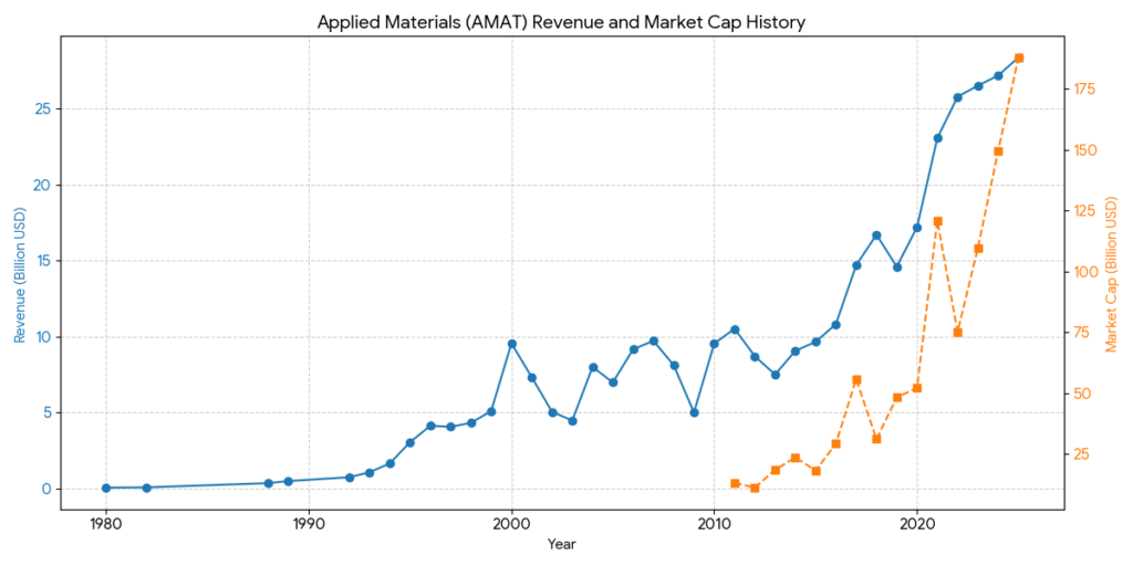
Applied Materials’ journey reflects the evolution of the semiconductor industry, transforming from a small chemical supplier into the world’s largest provider of wafer fabrication equipment.
Phase 1: Foundation & Early Struggle (1967–1975)
Founded in 1967 by Michael McNeilly, the company initially focused on chemical vapor deposition (CVD) equipment.
- 1967: Company founded in Mountain View, California.
- 1972: Applied Materials went public (IPO).
- Challenges: The company over-diversified into unrelated businesses, leading to financial instability and a near-collapse during the mid-70s recession.
Phase 2: The Morgan Turnaround & Core Focus (1976–1980s)
James Morgan took over as CEO in 1976 and implemented a “Back to Basics” strategy, shedding non-core assets to focus solely on semiconductor manufacturing.
- Global Expansion: Morgan recognized the importance of the Asian market early, establishing Applied Materials Japan in 1979.
- Technological Breakthrough: In 1981, the launch of the Precision Etch 8100 revolutionized the industry.
- The Precision 5000 (1987): This was a landmark moment. It introduced the multi-chamber platform, allowing different processes to happen in one vacuum system, significantly increasing yield and efficiency. It is now in the Smithsonian Institution.
Phase 3: Global Dominance & Expansion (1990s–2000s)
The explosion of the PC and internet era drove massive demand for chips, propelling AMAT to the top of the industry.
- 1992: Applied Materials became the world’s largest semiconductor equipment manufacturer.
- Diversification into Display: In the early 90s, they entered the Flat Panel Display (FPD) market, applying their vacuum deposition expertise to screens for laptops and TVs.
- Strategic Acquisitions: They expanded their portfolio through M&A, entering the metrology and inspection markets (Opal and Orbot) and the ion implantation market (Varian Semiconductor).
Phase 4: The Materials Engineering Era (2010–2020)
As Moore’s Law became harder to maintain, the industry shifted from simple scaling to complex “Materials Engineering.”
- 2011: The acquisition of Varian Semiconductor for $4.9 billion solidified their lead in ion implantation.
- Beyond Silicon: AMAT began focusing on new materials like Cobalt and Ruthenium to solve the electrical resistance problems in shrinking chips.
- Service & Software: Under CEO Gary Dickerson, the company shifted toward “Applied Global Services” (AGS), providing data-driven maintenance and software to optimize fab performance.
Phase 5: AI, Power, & Advanced Packaging (2021–Present)
Today, AMAT is positioned at the intersection of AI, energy efficiency, and heterogeneous integration.
- The PPACt Playbook: AMAT focuses on Power, Performance, Area-Cost, and Time-to-market.
- Advanced Packaging: As traditional scaling slows, AMAT is leading in “Heterogeneous Integration,” providing tools for 3D chip stacking and hybrid bonding.
- AI-Driven Fabs: Utilizing AI to monitor and adjust manufacturing processes in real-time to increase throughput.
Competitive Landscape Analysis (2026 Perspective)
Applied Materials (AMAT) operates in the Wafer Fabrication Equipment (WFE) market, which is characterized by high R&D costs and extreme technical barriers. In 2026, the competition has shifted from simple “transistor shrinking” to “3D structures and AI-driven performance.”
1. The “Big Five” Market Map
AMAT is the most diversified player among the five titans that dominate ~70% of the market. Its competitors specialize in specific niches where they often hold a technical edge:
- ASML (The Lithography Monolith):
- Focus: Photolithography (EUV/DUV).
- Competition: AMAT doesn’t make scanners, but its Centura Sculpta (pattern-shaping tool) directly competes for “wallet share” by allowing chipmakers to bypass some of ASML’s expensive EUV double-patterning steps.
- Lam Research (The Etch Specialist):
- Focus: Dry Etch and Deposition.
- Competition: Lam is AMAT’s fiercest rival in 3D NAND and HBM (High Bandwidth Memory) production. Lam’s “Cryogenic Etching” technology is a major threat to AMAT’s etch market share in the latest memory architectures.
- Tokyo Electron (TEL – The Track Leader):
- Focus: Photoresist Coaters/Developers and Thermal Processing.
- Competition: TEL dominates the “Track” market (tools connected to ASML scanners). They compete head-to-head with AMAT in ALD (Atomic Layer Deposition) and cleaning technologies.
- KLA (The Gatekeeper of Yield):
- Focus: Metrology and Inspection.
- Competition: While AMAT has an inspection business (e.g., eBeam technology), KLA remains the gold standard. As 2nm processes become standard in 2026, KLA’s ability to find atomic-level defects is the primary hurdle for AMAT’s process tools.
2. Strategic Competitive Advantages
- Breadth of Portfolio: AMAT is the only company that can provide an “Integrated Materials Solution.” They can combine deposition, removal, and modification on a single platform (like the Endura platform), which reduces contamination and speeds up the production cycle.
- GAA (Gate-All-Around) Transition: As the industry moves to 2nm, the architecture of transistors is changing. AMAT’s leadership in selective epitaxy and AL-D gives it a “first-mover” advantage in providing the materials needed for these complex 3D structures.
- Advanced Packaging (The New Frontier): With the rise of AI, chips are being stacked (Chiplets). AMAT is leading in Hybrid Bonding and Through-Silicon Via (TSV) tools, which are essential for making NVIDIA-class AI GPUs and HBM3e/HBM4 memory.
3. Comparison Table (2025-2026 Market Dynamics)
| Company | Core Dominance | AI/2nm Strategy | Key Vulnerability |
| AMAT | Materials Engineering | Leading in Gate-All-Around (GAA) & Advanced Packaging | High exposure to China export regulations |
| ASML | Lithography (EUV) | High-NA EUV for <2nm nodes | Extreme complexity/cost of next-gen machines |
| Lam Research | Etching & Deposition | Dominating HBM stacking & 3D NAND | More sensitive to memory market cycles |
| TEL | Coater/Developer | Synergies with ASML; strong in Japan/China | Facing intense pressure from US competitors |
| KLA | Inspection/Yield | Essential for 2nm & 3D chip verification | Narrower focus compared to AMAT’s “all-in-one” |
4. 2026 Market Outlook
According to recent industry reports, the “AI-driven Capex” is benefiting AMAT and Lam Research disproportionately due to the massive demand for HBM and advanced packaging. While ASML remains the “king of lithography,” Applied Materials is currently seen as the “king of materials,” capturing a larger slice of the value created by new transistor architectures.
Source:
- https://ir.appliedmaterials.com/news-releases/news-release-details/applied-materials-announces-fourth-quarter-and-fiscal-year-2025/
- https://www.macrotrends.net/stocks/charts/AMAT/applied-materials/revenue
- https://www.macrotrends.net/stocks/charts/AMAT/applied-materials/market-cap
- https://www.appliedmaterials.com/us/en/blog/blog-posts/a-deeper-look-into-the-new-vistara-platform.html
- https://ir.appliedmaterials.com/static-files/af687923-06c7-4b43-a7a5-45750717f3ca
- https://www.einpresswire.com/article/898665692/front-end-semiconductor-equipment-market-2026-boosted-by-precision-wafer-processing
- https://www.kavout.com/market-lens/tokyo-electron-toely-vs-u-s-competitors-who-leads-in-the-semiconductor-race
- https://en.eeworld.com.cn/mp/XSY/a350129.jspx
Back to Applied Materials page