Here is the history of Micron Technology, organized by developmental stages:
Phase 1: Founding and Early Breakthroughs (1978 – Early 1980s)
Micron was founded in 1978 in the basement of a dental clinic in Boise, Idaho. Originally a semiconductor design consulting firm, it quickly pivoted to manufacturing.
- 1978: Founded by Ward Parkinson, Joe Parkinson, Dennis Wilson, and Doug Pitman.
- 1981: Completed its first wafer fabrication plant (Fab 1) and began producing 64K DRAM chips.
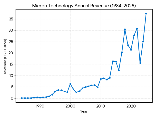
- 1984: Went public on the NASDAQ (IPO). That same year, it introduced the world’s smallest 256K DRAM chip, establishing its reputation for cost efficiency and technical miniaturization.
Core Technologies
- Focused on DRAM miniaturization, developing the world’s smallest 256K DRAM at the time.
- Centered R&D on “chip size minimization” to establish a low-cost manufacturing advantage.
Revenue Levels
- Annual revenue was approximately $84 million at the time of its 1984 IPO.
- Operates as a startup with revenue in the millions to hundreds of millions of dollars.
Phase 2: Diversification and Rapid Expansion (Mid-1980s – Late 1990s)
Despite intense competition from Japanese semiconductor firms, Micron solidified its position through innovation and strategic acquisitions.
- 1994: Entered the Fortune 500 list.
- 1998: Executed a major opportunistic acquisition by purchasing Texas Instruments’ (TI) worldwide memory operations, significantly increasing its global footprint and production capacity.
- Product Expansion: Introduced the industry’s first DDR DRAM in 1999 and began expanding into NAND flash and CMOS image sensors.
Core Technologies
- Launched the industry’s first DDR DRAM, setting the standard for computer memory.
- Acquired Texas Instruments’ (TI) memory division, gaining global production layout and advanced process technologies.
- Expanded into NAND Flash and CMOS image sensor sectors.
Revenue Levels
- Entered the Fortune 500 in 1994; revenue surpassed $2.95 billion in 1995.
- Revenue officially scaled into the billions of dollars.
Phase 3: Transition and Global Integration (2000s)
As the mobile and internet era emerged, Micron shifted its focus from PC memory to a broader range of storage solutions.
- 2005: Formed IM Flash Technologies, a joint venture with Intel focused on NAND flash memory.
- 2007: Established an assembly and test facility in Xi’an, China, accelerating its global supply chain layout.
- 2010: Acquired Numonyx, a manufacturer of NOR flash memory, further rounding out its storage product portfolio.
Core Technologies
- Formed a joint venture with Intel (IM Flash) to develop NAND Flash for the non-volatile storage market.
- Developed LPDRAM (Low Power DRAM) for mobile devices to meet early smartphone demand.
- Acquired Numonyx to master NOR Flash technology, completing its storage product portfolio.
Revenue Levels
- Revenue reached $6.36 billion in 2000 but fluctuated significantly due to the dot-com bubble.
- Impacted by the global financial crisis, revenue retracted to approximately $4.8 billion in 2009.
Phase 4: Consolidation and Technical Leadership (2010s – Early 2020s)
During this stage, Micron acquired struggling competitors to become one of the top global memory giants, forming a dominant trio alongside Samsung and SK Hynix.
- 2013: Acquired Japan’s Elpida Memory, making Micron the world’s second-largest DRAM supplier and securing a key spot in Apple’s supply chain.
- 3D Technology Breakthrough: Collaborated with Intel in 2015 to launch 3D NAND and 3D XPoint technologies, pivotal shifts in storage architecture.
- 2020: Led the industry by mass-producing 176-layer 3D NAND, demonstrating superior R&D capabilities.
Core Technologies
- Mastered 1α and 1β DRAM processes, leading competitors into mass production.
- Achieved breakthroughs in 3D NAND stacking, successfully mass-producing 176-layer architectures.
- Acquired Elpida Memory, gaining advanced Mobile DRAM technology and entering Apple’s supply chain.
Revenue Levels
- Recorded a milestone revenue of $30.4 billion in 2018, driven by a memory market bull run.
- Solidified its position as a top-three global memory giant, turning profitable with significantly improved gross margins.
Phase 5: AI-Driven Growth and Onshoring (Mid-2020s – Present)
Driven by the AI boom and geopolitical shifts, Micron has pivoted toward high-value AI applications and domestic US manufacturing.
- 2022: Launched the advanced 1-Beta DRAM node and 232-layer NAND. Announced massive investment plans for new fabs in New York and Idaho, supported by the CHIPS Act.
- 2025: Set record annual revenue driven by High Bandwidth Memory (HBM) for data centers and AI. In December 2025, the company announced its exit from the retail consumer brand business (Crucial) to focus entirely on the high-margin enterprise and AI markets.
Core Technologies
- HBM3E and HBM4 (High Bandwidth Memory) became the compute core for AI servers.
- Mass production of 232-layer and above 3D NAND to meet AI data storage needs.
- Introduced 1γ (1-gamma) process utilizing EUV (Extreme Ultraviolet) lithography to push process limits.
Revenue Levels
- Achieved record-breaking annual revenue of $37.4 billion in fiscal year 2025.
- Q1 FY2026 quarterly revenue reached $13.6 billion, with AI-related products (like HBM) serving as the primary growth engine.
As of early 2026, Micron Technology’s competitive landscape is defined by its strong pivot from a traditional commodity memory supplier to a high-margin AI enabler.
Market Share and Strategic Positioning (2026)
Micron currently maintains a solid position among the “Big Three” memory giants. While it remains the third-largest DRAM supplier overall, it has achieved a strategic breakthrough in the High Bandwidth Memory (HBM) segment.
- HBM Market Shift: As of mid-2025, Micron successfully overtook Samsung to become the second-largest HBM provider with a 21% market share, trailing only SK Hynix (62%).
- Product Allocation: Micron’s entire HBM supply for the 2026 calendar year is already sold out, indicating extremely high demand and strong customer lock-in with major AI players like NVIDIA and AMD.
- Customer Base: Micron is a primary supplier for NVIDIA’s Blackwell GPU architecture (including H200 and B200) and AMD’s Instinct MI300 series.
Technical Competitive Advantages
Micron’s “Value over Volume” strategy is centered on energy efficiency and rapid node transitions.
- Power Efficiency Leadership: Micron’s HBM3E chips are noted for having approximately 30% lower power consumption than those of its nearest competitors, a critical factor for AI data centers struggling with thermal management.
- HBM4 Progress: Micron is on track to ramp up HBM4 production in the second quarter of 2026. These chips feature data speeds exceeding 11 Gbps and are developed using advanced in-house CMOS and metallization processes.
- DRAM Node Dominance: Micron has led the industry for four consecutive technology nodes (1-alpha through 1-gamma). Its 1-gamma DRAM, which utilizes Extreme Ultraviolet (EUV) lithography, is expected to become the majority of its bit output by late 2026.
Competitor Dynamics
- SK Hynix: Remains the market leader and NVIDIA’s most entrenched supplier. Their competitive edge lies in their specialized packaging technologies (MR-MUF) and long-standing partnership with AI leaders.
- Samsung Electronics: Despite falling into third place in the HBM market during 2025, Samsung is aggressively investing in its HBM4 roadmap. They aim to regain share in 2026 by leveraging their “One-Stop Shop” model (combining memory, foundry, and packaging).
Financial Resilience and Growth
- Revenue Performance: Micron reported record revenue of $13.6 billion in FQ1 2026 (a 57% YoY increase). Analysts project 2026 revenue could surge by over 90% as the “AI supercycle” continues.
- Profitability: Gross margins have expanded significantly (reaching approximately 67% in recent guidance) due to the higher price-per-bit of HBM compared to standard DDR4/DDR5 memory.
- CapEx Strategy: Micron has increased its 2026 capital expenditure plan to approximately $20 billion, prioritizing HBM capacity and 1-gamma output at facilities in the U.S. (Idaho, New York), Japan, and Singapore.
Here is the detailed technical comparison between Micron and SK Hynix regarding their HBM4 (6th generation High Bandwidth Memory) developments, as of January 2026.
Micron vs. SK Hynix: HBM4 Technical Specification Comparison
| Feature | Micron Technology | SK Hynix |
| I/O Interface | 2048-bit (JEDEC Standard) | 2048-bit (JEDEC Standard) |
| Per-pin Speed | >11 Gbps (Industry-leading) | 10 – 11.7 Gbps |
| Total Bandwidth | 2.8 TB/s per stack | ~2.0 – 2.5 TB/s per stack |
| Stacking Height | 12-High (36GB) initially | 12-High (36GB) & 16-High (48GB) |
| DRAM Node | 1-beta (1β) / 1-gamma (1γ) | 1-beta (1b) |
| Base Die Logic | TSMC 12nm / 5nm Custom | TSMC 12nm / 5nm Alliance |
| Packaging Tech | Advanced TC-NCF | Advanced MR-MUF |
| Power Efficiency | ~30% improvement vs HBM3E | ~40% improvement vs HBM3E |
| Mass Production | Q2 2026 | Q1 2026 (Early ramp) |
Core Technology & Strategic Differentiation
1. Performance and Bandwidth Leap
Micron has made a significant statement by achieving 11 Gbps per-pin speeds, resulting in a total stack bandwidth of 2.8 TB/s. This surpasses the standard JEDEC HBM4 baseline (8 Gbps / 2.0 TB/s). While SK Hynix has demonstrated speeds up to 11.7 Gbps in lab settings, Micron’s focus is on maintaining this 11 Gbps performance at high yields for 2026 mass production.
2. Stacking Technology: MR-MUF vs. TC-NCF
- SK Hynix (MR-MUF): SK Hynix continues to refine its Mass Reflow Molded Underfill (MR-MUF) process. This technology is highly effective for heat dissipation and is the reason SK Hynix was the first to successfully demonstrate a 16-High (48GB) HBM4 stack at CES 2026. This gives them a capacity edge for ultra-high-end AI servers.
- Micron (TC-NCF): Micron utilizes Thermal Compression Non-Conductive Film (TC-NCF). While historically perceived as more difficult for high-layer counts, Micron’s proprietary CMOS-based die innovations allow for thinner wafers (reducing thickness while maintaining structural integrity). Micron emphasizes that its implementation offers the best-in-class power efficiency, which is critical for reducing the Total Cost of Ownership (TCO) in massive AI clusters.
3. The “Base Die” Revolution
HBM4 marks the first time memory makers are integrating logic processes into the base die:
- The TSMC Alliance: Both companies have partnered with TSMC to utilize 12nm and 5nm nodes for the base logic die. This allows the HBM4 to act more like a “logic chip,” enabling features like Custom HBM, where the memory can be tailored specifically for NVIDIA’s Rubin or AMD’s Instinct platforms.
- Micron’s Edge: Micron’s HBM4 features specialized built-in self-test (MBIST) technology, allowing for faster and more reliable system-level verification, which is a key requirement for NVIDIA’s high-yield requirements.
4. Market Readiness (2026 Roadmap)
- SK Hynix remains the volume leader, with its HBM4 mass production system established in late 2025 and early shipments ramped for Q1 2026. They are currently the primary supplier for NVIDIA’s early Rubin samples.
- Micron is positioned as the “performance and efficiency” alternative. Having shipped 12-High samples in 2025, Micron is on track for a high-yield ramp in Q2 2026. Notably, Micron has already sold out its entire 2026 HBM capacity, underscoring its successful capture of market share.
Summary of Competitive Edge
- Choose SK Hynix for: Maximum stack density (16-High) and proven high-volume reliability through their MR-MUF expertise.
- Choose Micron for: Industry-leading bandwidth (2.8 TB/s) and superior power efficiency that helps mitigate the massive energy demands of AI data centers.
Source:
- https://www.investing.com/news/swot-analysis/micron-technologys-swot-analysis-stock-soars-on-aidriven-memory-demand-93CH-4278521
- https://www.astutegroup.com/news/general/sk-hynix-holds-62-of-hbm-micron-overtakes-samsung-2026-battle-pivots-to-hbm4/
- https://investors.micron.com/static-files/530bd7ed-a8c8-4687-af4a-8c129f740e09
- https://www.zacks.com/stock/news/2819366/nvidia-vs-micron-which-ai-chip-stock-is-a-better-investment-option
Back to Micron page