The history of ASML is a journey from a struggling joint venture to becoming the most critical company in the global semiconductor supply chain.
Here are the key stages of ASML development:
1. The Survival Era(1984-1990)
- Foundation: ASML was founded in 1984 as a joint venture between Philips and ASM International(ASMI). They started in a leaky shed in Veldhoven, Netherlands.
- The Struggle: At that time, Japanese giants Nikon and Canon dominated the market. ASML had almost no customers and faced constant financial crises, surviving only through continuous funding from Philips.
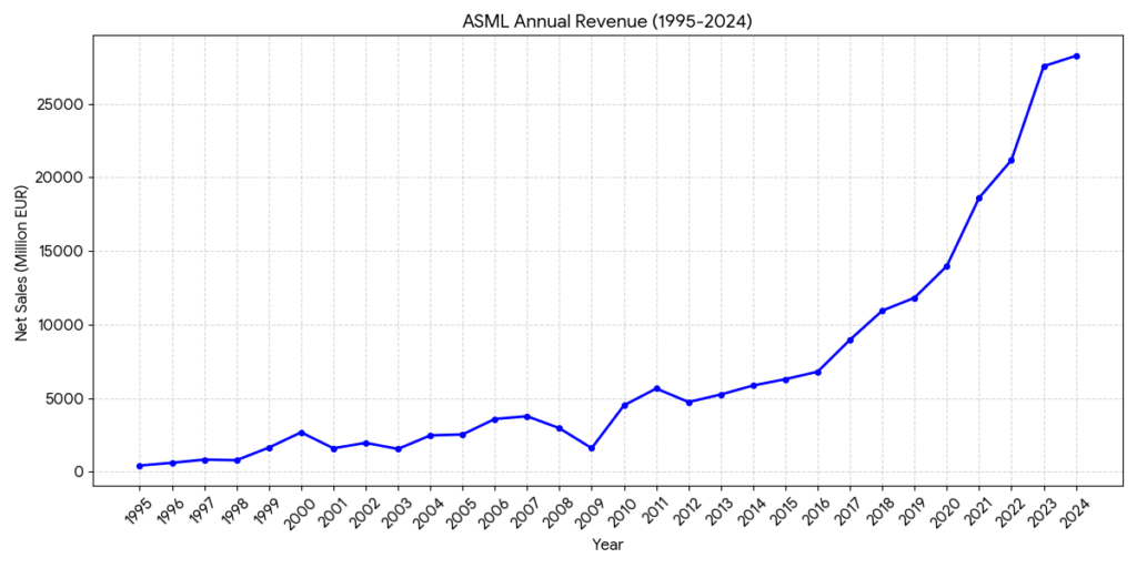
Revenue Level: Extremely low and loss-making. Starting with a few million dollars in seed capital, the company often sold fewer than 10 units per year. It survived primarily on subsidies from Philips.
Core Technology: Stepper Lithography.
- PAS 2000/2500: Utilizing alignment technology from the PCB industry. While less precise than Japanese competitors at the time, it established the foundation of Modular Design, allowing for faster repairs and upgrades.
2. Market Entry and IPO(1991-2000)
- The PAS5500 Breakthrough: Launched in 1991, this machine became the industry standard due to its modular architecture and productivity. It allowed ASML to finally compete with Japanese rivals.
- Going Public: In 1995, ASML listed on the Amsterdam and NASDAQ stock exchanges, providing the capital needed for massive R&D.
- Acquisition: In 2001, ASML acquired Silicon Valley Group(SVG), gaining a stronger foothold in the US market.
Revenue Level: Revenue grew from approximately 100 million EUR to over 1.5 billion EUR. The 1995 IPO provided the capital for rapid global expansion.
Core Technology: PAS 5500 Platform & Twinscan.
- i-Line & KrF (248nm): The PAS 5500 became a legendary industry workhorse due to its high throughput.
- Twinscan (Dual-Stage): Introduced in 2000, this allowed one wafer to be measured while another was being exposed, doubling productivity and becoming ASML’s signature competitive advantage.
3. The Immersion Revolution(2001-2010)
- The Strategic Bet: While competitors like Nikon focused on 157nm dry lithography, ASML bet on Immersion Lithography(using water as a lens) after collaborating with TSMC Burn-Jeng Lin.
- Market Leadership: The Twinscan immersion systems were a massive success, allowing chipmakers to shrink features to 45nm and beyond. By 2006, ASML had officially overtaken Nikon as the market leader.
Revenue Level: Revenue climbed from 2 billion EUR toward 5 billion EUR. ASML captured over 80% of the high-end lithography market during this period.
Core Technology: ArF Immersion (193i).
- 193nm + Water Media: By placing a layer of deionized water between the lens and the wafer, ASML effectively shortened the wavelength, allowing features to shrink to 45nm and eventually 7nm (via multi-patterning).
- Multi-patterning: This technique extended the life of DUV (Deep Ultraviolet) machines far beyond what physics initially predicted.
4. The EUV Mastery(2011-2023)
- Extreme Ultraviolet(EUV): This technology uses light with a wavelength of 13.5nm. It was so difficult that many thought it was impossible.
- Customer Investment: In 2012, ASML invited Intel, TSMC, and Samsung to become shareholders and fund EUV development.
- Absolute Monopoly: ASML successfully commercialized EUV, becoming the world’s only supplier. This made them the gatekeeper for all advanced chips(7nm, 5nm, 3nm).
Revenue Level: Massive growth from 6 billion EUR to 27.6 billion EUR (2023). Gross margins rose above 50% as the company became a monopoly in advanced nodes.
Core Technology: Extreme Ultraviolet (EUV).
- 13.5nm Wavelength: Using CO2 lasers to hit tin droplets 50,000 times per second to create plasma.
- Reflective Optics: Since EUV is absorbed by glass, ASML and Zeiss developed the world’s flattest mirrors to guide the light. This technology is the only way to produce chips at 7nm, 5nm, and 3nm without extreme complexity.
5. High-NA and Geopolitics(2024-Present)
- High-NA EUV: ASML is now deploying the next generation of machines, High-NA EUV, which are required for 2nm processes and below. These machines cost over 350 million USD each.
- Strategic Asset: Because its technology is indispensable, ASML has become a focal point of global trade tensions and export controls.
Revenue Level: 2024 revenue was approximately 28.2 billion EUR. Forecasts for 2025/2026 range between 30 billion and 35 billion EUR, driven by the AI chip boom.
Core Technology: High-NA EUV (0.55 NA).
- Anamorphic Lenses: A new lens system that increases the Numerical Aperture (NA) from 0.33 to 0.55, enabling much higher resolution for sub-2nm nodes.
- Hyper-Cost Hardware: These machines cost over 350 million USD each and are roughly the size of a double-decker bus.